
What are
/r/FPGA's
favorite Products & Services?
From 3.5 billion Reddit comments
The most popular Products mentioned in /r/FPGA:


The most popular Services mentioned in /r/FPGA:
Hackster
Amazon Elastic Compute Cloud
HackADay
Digital
Hacker News
Udemy
Linux kernel
Vim
Notion
Google Drive
Google Groups
8bitworkshop
hastebin
Overleaf
Stack Overflow
The most popular VPNs mentioned in /r/FPGA:
The most popular reviews in /r/FPGA:
PYNQ is your friend here, I am literally just working on a hackster project which shows how you can use PYQN and openCV to test out your algorithm. Then you can use the XF:openCV / Vitis Vision libraires in HLS to accelerate and run them through the hardware.
Creating new overlays is actually simpler than creating solutions which are going to use Petalinux.
I did a recent PYNQ course which is available for free online the link is here https://www.adiuvoengineering.com/post/microzed-chronicles-free-virtual-workshops-on-demand
The project I am doing will be on hackster in the next day or so, there are several other image processing ones there as well my channel is https://www.hackster.io/adam-taylor
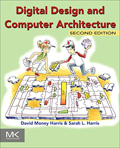
https://www.amazon.com/Digital-Design-Computer-Architecture-Harris/dp/0123944244
This book teaches you how to implement a 32-bits MIPS processor with single or multi-cycle design using verilog.
Check out the Amazon Cloud AWS F1 gives you a good opportiunity to do exactly what you want. I did a tutorial on this recently https://www.hackster.io/adam-taylor/using-aws-f1-fpga-acceleration-d5563b
Bebop to Boolean Boogie is pretty good. Very easy and fun book to read. Covers a ton of great entry level topics.
Then move towards something more FPGA specific like
~~Knowing C will probably hurt you more than help you. Forget what you know about C when learning Verilog.~~ You need to approach learning Verilog in a different manner. Verilog is not another top-down procedural language expressing instructions one after another. There are some general programming tenets that still hold true, and attention to detail in regards to syntax is important. But forget about line-by-line procedural execution because that's not how these hardware description languages work. You need to learn DIGITAL DESIGN before you learn Verilog....
EDIT: for clarity and to tighten up my thoughts.
My favourite textbook is Uwe Mayer-Baese, 'Digital Signal Processing with Field Programmable Gate Arrays'
https://www.amazon.com/Digital-Processing-Programmable-Communication-Technology/dp/3642453082
I've implemented FFTs, FIRs and DDCs in a Spartan-3a DSP board, running real time with a sampling rate of 70MS/s. To a large extent, that meant using ready-made modules from Xilinx that already ship with the design software. Study the manual that comes with these blocks really carefully, but for my application, they just worked. The blocks aren't all that specific to your device, but are quite vendor specific, although each of the vendors have their own version of them.
You know Xilinx has a range of OpenCV cores which are HLS capable?
https://github.com/Xilinx/xfopencv
see my own example here
https://www.hackster.io/adam-taylor/fpga-based-edge-detection-using-hls-192ad2
I would recommend you the book SystemVerilog for Verification.
According to Xilinx, you can run UVM testbenches on Vivado 2019.1. I'm using 2020.1 version and constrained random generation is working well.
Cool, I will fork your project and must be able to learn something from it.
I used to be a software developer, I actually don’t know much on hardware design process. Thanks for being welling to help, it is good to know I can get some help from people with experience.
BTW, here is my GitHub and devlog https://github.com/fallingcat
https://www.notion.so/fallingcat/Homebrew-GPU-Project-3b5ca66a3b4b45039941995a8f82f89b
>Can you give me any more to lead me down the right path? Like how I would start thinking about taking data encoded in a certain format (like JSON) and decoding it into another format?
You are so far from the point where this is the question you should have.
Questions about FPGAs you should be asking right now:
- Which HDL should I learn?
- How do I set-up a board so I can get an LED to blink.
- How do I write code to get a seven-segment display to show the state of four dip switches in hex?
- How do I do 3, but with binary coded decimal?
- How do I write a state machine in my chosen HDL?
- How to I write a I2C interface?
Then we can address the next set of questions. JSON means nothing to an FPGA, and human readability of the data you're sending to it has got to be the worst possible way to think about sending data to an FPGA. FPGAs and CPLDs are often used as "glue logic" to tie two interfaces together. So it's something they can do. JSON is just a very weird format to choose.
Seriously, check out this. HDLBits, Nand2Tetris. When working with FPGAs you need to realize that you're literally describing the hardware that the FPGA will implement. Like, imagine setting up a series of logic gates to decode JSON into a different format. If the scale of that problem doesn't terrify you, you need to start at the beginning.
The slides from Unallocated Space's FPGA class might help you. They are meant for people who don't have any experience with FPGAs. Check out Google Drive to see all the slides.
It is pretty easy and straight forward to add a SPI flash to your FPGA board. You find really cheap items at AliExpress ! You can also add a SD-Card Pmod and store your data on a SD card you can find the board at Digilent, they also have good examples you can use in your design.
This stack overflow page gives a pretty complete overview. The TLDR is either use the ieee.numeric_std operators, or build your own n-bit shifter that performs a concatenation op:
sig(n downto 0) <= sig((n - 1) downto 0) & '0';
EDIT: correctly summarized the article.
Another great book (this is the RISC-V Edition, but you also have the classic MIPS edition) :
I recently had a book come out on SystemVerilog if this might be of interest:
I'm a bit biased :) but I wrote it from 30 years experience for people new to hardware. It covers all (most?) of the gotchas that people unfamiliar with designing hardware will face.
OP here I had not seen these other projects of yours somehow. Very nice. I really appreciate the contribution you (and presumably friends) made with Yosys and the continued effort you are putting into opening up this important area.
If you have any ideas or criticisms of what little bit of my plan I put forward in the post, I would be happy to know. I am still figuring out the extents of the project.
I will certainly review your implementation of the XPCUSB firmware.
There are many good comments here https://news.ycombinator.com/item?id=9408881
Also I believe you have been in contact with some of thew IRC friends I alluded to in the post. If so, thanks for the help you gave them.
Bruce Land is a teacher whose students make lots of interesting projects, he has two groups on Facebook about FPGAs and here you can see an example of a project from his students that is somehow related to what you are asking http://hackaday.com/2016/06/16/no-frame-buffer-for-fpga-vga-graphics/
Yes, that was the problem, thank you!
It still baffles me that people use different webserver endpoints for HTTPS and HTTP requests. Literally everything should be HTTPS these days!
HTTPS Everywhere is still a great extension though. I would highly recommend it to anyone.
I couldn't find a test bench. I have read the data sheet a few times. I doesn't say anything about timing. The timing diagrams show multiple writes where the write signal remains high. It's synchronous so it just samples the data each clock cycle, so leaving the write signal high makes sense so I tried doing that as well without any luck.
Here's a link to my (very simple) test.
Here’s a complete (I think) list of supported languages. I don’t see any HDLs listed. Others have asked this question before on this sub with more feedback from the folks who took the tests and can be found with a Google search.
And a connected recent piece of news: "Morten Shearman Kirkegaard and Peter Wilhelmsen (recently featured here in connection to their success in dumping Gaelco protection programs) have built another FPGA-based rig that allowed them to dump the internal programs from the ARM CPUs for Oriental Legend 2 and Knights of Valour 2 New Legend."
Hello, go to udemy.com and for a small amount about you can get course on Xilinx Vivado, HLS, AXI and Video Processing. There is also courses on verilog. They usually have sales throughout the month for $12. Also, check out Adam Taylor's blog site.
You are right I recently posted a few examples how to do this on Hackster.
https://www.hackster.io/adam-taylor/use-python-zynq-and-opencv-to-implement-computer-vision-361e1b
https://www.hackster.io/90432/programming-python-on-zynq-fpga-ec4712
> Based on data of actual T2, not the synthesized version
I don't get what this means. (At least you are starting to give enough information that /u/OhhhSnooki can help you along.)
Have you seen https://www.slideshare.net/DVClub/opensparc-on-fpgas
This seems to be the OpenSparc T1. Note that slide 16 says something about "50% reduction in area" which seems to mean they threw half the design over the side. They fit whatever-it-is-that-was-left into some reasonable fraction of a XC5VLX110T.
I have got Zybo, Zedboard, MiniZed and Pynq V2 for Xilinx FPGA's. Today I prefer to work on the Pynq for the available hw interfaces. You could also look at the Ultra96 board but this is more expensive.
You should install the tools under Linux for the petalinux tools etc.
Just for your reference I think this book will be perfect to learn about CPU design (there is a ARM and RISCV version available) : https://www.amazon.com/Digital-Design-Computer-Architecture-RISC-V/dp/0128200642 I did the ARM edition.
You can get a cheap entry level board (like the nandland Go) for $65. That's a hell of a lot of capability for a cheap price.
You can even get a bit cheaper than that if you're willing to buy peripherals as you go. The Waveshare Cyclone IV boards are like $35 ($43 with a USB programmer).
Yes 2.0 just refers to it being USB 2.0 compatible. This cable would work for you: https://www.amazon.com/UGREEN-Adapter-Samsung-Controller-Android/dp/B00N9S9Z0G
OTG or "on-the-go" is just a spec where USB devices could also operate in host mode to allow other devices to be attached to itself. For example, most modern Android phones can be plugged into a computer to transfer data but also can accept one of these OTG cables to allow you to plug in a flash drive directly to the phone.
To that end, I imagine the SoCKit has the same capabilities. They can be connected to a PC to communicate that way, or allow peripherals like flash drives to be attached using an OTG cable.
The link to the book is here. It's a one-of-a-kind given how uncommon VLSI is.
The best starting point is Clifford Cumming's CDC paper. It's a very widely read paper in the industry.
https://smile.amazon.com/Computer-Organization-Design-RISC-V-Architecture/dp/0128122757
Just start writing the HDL. Put it on an FPGA.
Ha yep, the one with the VGA. Here's the textbook I bought: https://www.amazon.com/dp/0262042649?ref=ppx_pop_mob_ap_share
I haven't ever read another one, so I don't have anything to compare it to but I thought it was very informative and interesting.
Okay I've worked on some stuff and in my testbench sims the output works but when i run my program the keyboard doesn't seem to be outputting anything. Could it be an issue with my keyboard itself? Its new and i got it for this project, its a https://www.amazon.com/dp/B00JV08TIA?psc=1&ref=ppx_yo2ov_dt_b_product_details. The lights in the corner don't turn on so could it not be getting power from the DE2? It doesn't have any other power connections so I'm not sure how it would be powered otherwise.
I did only take a really quick look. The high level diagram lists D[35] into the "Video Data Capture" and then probably need 5 ish pins for everything else, so I went with ~40. If the I/O is differential, then 16bits require 32 pins.
If you only need ~19 per ADV7511 then you could easily dump two of these onto a TOFE board to interface with the Opsis. I recon you could do that board in individual quantities for under $100 USD without any trouble at all. It seems within possibility to even get it under $50 USD for individual quantities if you are careful (thanks to the low cost of doing TOFE boards).
If you are interested in actually doing such a board and have the time, I'd love to work with you on it (I may even get you an Opsis and fund the prototype run). Feel free to contact me on or just propose it on the hdmi2usb mailing list.
My desk right now is covered with hand-drawn timing diagrams. I found a PDF of 11x17 graph paper and printed a whole bunch.
When I was in college, I worked for the school's publications department doing paste-up of mechanicals that were sent off for printing (and this outs my age, kids, get off my lawn while I listen to my OG copy of "Bad Moon Rising" by Sonic Youth) and I got indoctrinated into the world of Mars-Staedler and their amazing erasers and mechanical-drawing pencils and that's all I use.
That shit's expensive but soooo worth it. Also expensive but worth it are the Ampad green engineering paper pads which don't come in sizes other than Letter (A) (sad face).
Anyway, The Point:
It really helps to know what you're trying to implement before you start typing a bunch of HDL.
And yes, I've tried every timing diagram drawing program out there, and I always come back to the pencil and quadrille paper.
Sounds like cool stuff.
For Zynq specifics and great examples on using Vivado for Zynq SoC development, have you seen the Zynq Book? There is a lot of great information in there.
For bottom up courses on FPGAs I'm not super familiar with any. A great text book which simply covers introductory details on hardware design, FPGAs, and hardware description languages is Digital Design and Computer Architecture by Harris and Harris. Not all chapters of the book are relevant to what you're interested in, but some contain the introductory information I think you're looking for. If you're uninterested in paying for the book, it shouldn't be too difficult to find it online 😉.
re: Diamond vs Radiant, the difference is in device support.
Documentation for that board says it has the ICE40UP5K FPGA, so you need Radiant, and the Lattice web site says that the license that supports that device is free.
Assuming that the board's FTDI thing appears as a program to the Lattice tools, it should be fine. I have no direct experience.
Ages ago I bought a MachXO2 board to prove out a concept prior to committing to a product board design, and that worked well enough with the Diamond tools. Surprisingly, Newark has two in stock though the price is stupid.
So you already know how digital design works and just need a Verilog language guide. This might be what you are looking for: https://link.springer.com/book/10.1007/978-3-030-10552-5. Actually I would also recommend to read the standard: IEEE 1364. Another one often recommended is https://www.amazon.com/Verilog-Example-Concise-Introduction-Design/dp/0983497303.
So “faster” is some averaged packet arrival time that’s given/external to the problem statement?
What happens to the unselected stream? Dropped? Buffered?
Is out > 2x input clock? Or “fast enough given [expected] arrival times to not overflow “?
I would recommend effective coding with vhdl by ricardo jasinski.
https://www.amazon.com/Effective-Coding-VHDL-Principles-Practice/dp/0262034220
I also wrote about some practical ways to manage dependencies in shared code some time ago which you also might find useful.
Yeah that can work too.I wanted to do a digital clock for a school project using vhdl .In fact i found one board on amazon : spartan 6 - https://www.amazon.com/Xilinx-Development-XC6SLX9-Spartan6-easyFPGA-Spartan-6/dp/B098JNS1FG/ref=mp_s_a_1_6?crid=ZIY93XPFI8UH&keywords=spartan+6+fpga&qid=1650230319&sprefix=spartan+6+fpga%2Caps%2C207&sr=8-6 Is it worth to buy ?
Thanks! Quick link for others: https://www.amazon.com/Static-Timing-Analysis-Nanometer-Designs/dp/0387938192#aw-udpv3-customer-reviews_feature_div
In one of the review this one is suggested: Timing https://www.amazon.it/dp/1441954082/ref=cm_sw_r_awdo_F10DM52DMDPEK9DVHQJK
Recommended read: On the Origin of Circuits and this book.
Mentor Graphics verification academy, you'll need to create an account, and IIRC that requires a work / academic e-mail address. But then there's a few short videos that guide you through the basics. I've watched those and learnt a bunch, however they are not that extensive, you have to figure a bunch of stuff out for yourself.
I've also been recommended this book: https://www.amazon.com/Practical-Adopting-Universal-Verification-Methodology/dp/057805955X but I can't vouch for it.
I'm not sure of any other good ones. I've been doing things so long I don't typically read these types of books.
I don't have any particular recommendations for projects. If you have some example code in 'c' or similar it shouldn't be that hard to adapt to SystemVerilog once you know the basics. Feel free to PM me if you have any questions.
You may consider looking at Udemy.com they have some courses that may be beneficial:
Synthesizable SystemVerilog for an FPGA/RTL Engineer
Using Xilinx Vivado Design Suite 2020
ah OK. In my work we have a few boards that have a CPU of some type that runs linux and an FPGA that communicate over PCIe, so I kind of assumed you'd be in the same state.
Plus after a bit of thought, I think I was on the wrong track. I was assuming you wanted to know how to talk to the PCIe peripheral on your processor. Which you totally don't need to do (if you were thinking that). You just need to interface with the PCIe comms layer of linux. Which unfortunately I don't have any suggestions, other than find an existing driver and copy it with any relevant changes.
This looks interesting https://stackoverflow.com/questions/32592734/are-there-any-dma-driver-example-pcie-and-fpga
imo plan for getting into good eecs program in college... fpgas are college stuff...also companies hires college grads in this field..
as for packet filter... first get your hand dirty with pihole and raspberry pi
then go for
I did a blog on that here
https://www.hackster.io/news/microzed-chronicles-zynq-multiboot-and-in-the-field-update-a7aeda7c9d48
be very careful about ensuring the updated file is correct before you replace it
You might be interested in the discussions on the topic of master and slave terminology. There’s a Wikipedia page that lists a bunch of companies that have moved to newer terms for the same idea - it’s a surprisingly big list.
Some of the sources are links to discussions on change requests in different projects, where it’s talked about in depth as well and different opinions. I found the one from Drupal particularly interesting
If not I’m sure someone will see this post later. Thinking about bringing this up with my boss later, but I’m not sure yet.
Mermaid.js can describe FSMs in text. I've used it for other things, and it integrates into a ton of stuff that uses markdown. Might be worth a look if you want something simple.
A five-stage RISC-V pipeline with cache is a standard semester project for a group of 3-4 senior undergrad students. This is the standard textbook that walks through the course that typically accompanies the project. The course is typically called Computer Organization and Design as well.
​
The type of processor that AMD/Intel designs are incredibly complex in comparison. There is also a huge amount of work taking the design from synthesizable verilog that you run on FPGA to an actual ASIC. And verification, which is not typically done very well at the academic level. IMO, designing a simple core is a good, fundamental learning experience, but you'll learn much more from the "next steps" of adding advanced features, or adding the I/O and periphery that is expected of a processor.
Sounds like you're getting a processor-centric view. Three suggestions:
- Tomasulo's Algorithm is neat and all, but memory ordering is more important than is typically taught. (I think this is because it's possible to teach OoO looking at the CPU in isolation, but the memory subsystem is much more sprawling and complex.)
- The software side is increasingly exposed and increasingly important. The Linux kernel documentation on memory barriers is a well-written description of the impact reordering in silicon has on software.
- The "dark side" of all of this optimization is information leakage. Everyone wants faster processors, nobody wants it to impact security, and the chasm between these two desires runs black and deep.
Yea, I should have listed it in the first place. Haha. It is older, and I am still awaiting my hardcopy, but I have been reading a PDF. What I have read so far has been very helpful.
I'm not an expert in image processing, but your message excited me. I am an enthusiastic photographer and your problem is interesting. First of all, I think it would be interesting for everyone to know which camera you use? How can we influence the optical system?
As far as focusing methods are concerned, there are several. For example, you can directly measure the distance from the focal plane to the subject. Ultrasonic or infrared locators can be used here.
Contrast detection uses information directly from the light-sensitive element, reaching the maximum contrast between adjacent pixels. The optical system will be adjusted until the best contrast is obtained.
Phase detection is different and requires a separate sensor and is based on dividing the luminous flux into two images and finding the relationship between them.
When there is no possibility to influence the optical system, mathematical methods of blurred images recovery, such as the Wiener filter, are used. They use the convolution theorem and inverse filtering, as well as Point spread function information.
Forgive me for the terrible language, I am not a native English speaker and have to use a translator.
​
Translated with www.DeepL.com/Translator
This is a full example for Xilinx FPGA, not a theory book, but you'll certainly learn a ton if unfamiliar with FPGAs, SoC
https://www.hackster.io/adam-taylor/creating-a-zynq-or-fpga-based-image-processing-platform-e79394
Looks like the XPM way of creating BRAMs is more flexible and optimal.
https://www.hackster.io/news/microzed-chronicles-working-with-memories-cdc-structures-using-xilinx-parameterized-macros-b5abb0ea07cd
But it doesnt allow different widths for single port. BRAM Generator IP allows though.
The PicoBlaze tools are (unfortunately) rusting, and the principal engineer who built it has retired. I think there's an opportunity for someone to design and release a PicoBlaze replacement. The core is decent, but the tools aren't.
Presumably, you're interested in updating the PicoBlaze program without re-synthesizing the entire design. You can do this as follows:
- ensure your PicoBlaze takes instructions from an XPM that reduces down to a RAMB36 (not a RAMB18). This is oddly restrictive and required because updatemem is picky.
- synthesize the design into a bitstream.
You now have a .bit file with something in the instruction memory. To revise the PicoBlaze program:
- in Vivado, use write_mem_info to export your design's BRAM instances as a .mmi file
- regenerate your .mem info containing updated PicoBlaze code
- use updatemem to update the .bit file using the .mem and .mmi files
Updatemem produces a new .bit containing the old bitstream and new memory image. It only takes a few seconds (much better than a complete RTL-to-bitstream flow.)
This flow is documented here. I see /u/adamt99 has an article here, too.
Thanks for the reference you can find the list of all MicroZed Chronicles here
https://www.adiuvoengineering.com/microzed-chronicles-archive
you might be interested on my Hackster projects as well which are more completed projects opposed to concepts
I did a free course you can find here all about the Zynq, HW, SW and Linux https://www.hackster.io/workshops/minized?ref=workshops
There is my blog too and hackster projects, I will post a link to those once my new website goes up in the next few hours
Edit: the old nano soc had ~20k LE... Have to be careful to get the new version. More here:
http://hackaday.com/2015/06/13/two-new-dev-boards-that-wont-make-your-wallet-hurt-so-good/
Edit2: new version is the P0286 (The P0082 is the older Cyclone IV version): http://rocketboards.org/foswiki/view/Documentation/AtlasSoCEvaluationKit
Search for "Terasic Technologies P0286" on DigiKey or Mouser for details.
I wonder how the FPGA part stacks up to a spartan 6 (lx9 or better yet the lx45)? Edit: The Spartan 6 XC6SLX45 has around 43K "logic cells" versus the XC6SLX9 at 9K. Not sure "logic cells" map 1:1 to "logic elements" but if it does then the FPGA part is more like a Pipistrello (LX45) than a Papilio Pro or Mojo (LX9). I personally like (and own) the Papilio/Pipistrello boards, but I want to delve into the Altera side of things (and hey, SoC!)
Also, how limited is the software that is included? (Edit: guess I'll find out when my new board arrives!)
I've been pondering a switch myself... ISE is a dead end now (I don't think you can even install it on Windows 8 let alone 10) and thus I feel the Spartan 6 is not the way to go anymore. There are Zynx devices out there, and then you can use newer tools, but YMMV.
Yes that is a dataflow styled architecture as you have only used the single concurrent signal assignment statement "Y <= (A and B) or (B and C) or (A and C);".
A concurrent signal assignment statement is essentially describing the hardware implementation via gate logic, like you have done.
A concurrent process statement allows you to describe the behaviour like a typical software algorithm and will be used in behavioural styled architectures.
A concurrent structural process statement allows you to describe the behaviour as a hierachical system, where you can create instances of lower level design entities for the purpose of re-use and modularity of code.
If this is just for a module for your uni, I highly recommend this book:
https://www.amazon.co.uk/VHDL-Engineers-Pearson-New-International/dp/1292042753
You can find PDFs of it online if you search around for a bit.
Have you considered this?
It's a little bit awkward, but the way I understand it, you launch an EC2 instance with an FPGA development image. This image has special access to a couple of different FPGAs that are attached on "ports". You interact with the FPGA by sending it commands like "load this into your fabric" (called an AFI, which is analogous to an AMI for EC2). The tools to build an AFI are included in the FPGA development EC2 instance... so basically you do your Verilog or VHDL as you normally would, do your simulations and whatnot as you normally would, and then when you're ready to run on real hardware you build an AFI, push it to an FPGA with the command line tools, and then interact with the FPGA via other command line tools (like "show me your LED statuses" and stuff like that).
If your talking about Bluetooth Low Energy, It's actually even worse, 1Mb/s is the bit rate when transmitting, including headers and error correction. Bluetooth low energy does not transmit all the time, and the maximum packet length is quite short (27 bytes of data) so you have a lot of overhead.
The maths works out to 125Kbps Max throughput (see section data throughput).
If you can use something other than Bluetooth low energy, do. It's really not made for this at all, and its not like the low power matters when you have an FPGA there.
There is no need for a function-specific device driver unless you're integrating into the network stack or filesystem.
You do need one so that user-space apps can memory map the programmable logic, wait for interrupts, and share system memory with the hardware.
UIO is one way to do this: https://www.kernel.org/doc/htmldocs/uio-howto/about.html
Our project (http://www.connectal.org) uses a generic device driver that provides a common software interface to the programmable logic over zynq and PCIe attached programmable logic. It exposes multiple device nodes, in case you want to allow multiple processes to have independent access to functions on the programmable logic.
Have you downloaded the examples from this Terasic web site?
Apparently, the HPS (ARM core) has access to a UART interface.
There's an existing project located in the Terasic System CD:
TSOM_v.1.0.1_revB_SystemCD/Demonstration/Soc_FPGA/TSOM_GHRD/TSOM_top.qpf
The TSOM_top.sof programming file will allow you to run the demo (no need to rebuild).
Are you familiar with using the Quartus programming software?
Section 4.3 "UART to USB" in the Manual/TSoM_Evaluation Kit_User_Manual_revb.pdf file should point you in the right direction.
Do you have access to a USB Mini-B cable? Did the kit come with it?
If you don't have a terminal program already, I recommend PuTTY (for Windows) https://www.chiark.greenend.org.uk/~sgtatham/putty/latest.html
> There is a pretty complex encoding used on the wire for ethernet and honestly it would be best to use an off the shelf PHY or find an FPGA with one built in, if one exists.
I don't disagree. As the other person pointed out I skipped a skip regarding how the bits are modulated.
I got the impression OP was asking a "from scratch" method instead of using already-built libraries.
And thus any modem-like behavior (processing codes, flow control) would be done by the FPGA in terms of setting up a new internal module. My 1980s Hayes 4800 bps modem is all you'd have to mimic to get a solid IP layer negotiated.
I wouldn't call it <em>impossible</em> to build a modem solely with FPGA modules.
this paper shows how through polyphase decomposition and subsampling you can mimic the frequency conversion. IMPORTANT NOTE: all of its A-to-D components are outside of the FPGA.
Thank you. I tried logism and it seemed clunky so I searched for "logism alternatives" and found Digital at https://github.com/hneemann/Digital. I'm currently playing with Digital and plan on trying logisim-evolution a bit later.
I'm not mining. I'm attempting to bruteforce an ethereum wallet that is encrypted with scrypt. Currently Hashcat https://hashcat.net/hashcat/ does this using CPU only without the huge memory requirements that GPUS would need( 320GB per GPU), but the hashrate is very slow (25H/s on a 16 core Xeon workstation). I figured I could use FPGA to increase the core count / performance significantly.
Some companies use open-source tool to customize and organize their documentation but it involves a lot of effort from the technical team as well to set it up and maintain it.
Nowadays some top companies like Porsche, Harvard University, NHS use our product Document360 for creating, publishing, and maintaining their documentation.
Many saas product companies with more complex products are also satisfied with Document360.
Document360- #1 rated Knowledge base solution for creating technical docs.
Find out what our customers say about creating and maintaining documentation with us https://document360.com/customers/
Also have a look at http://8bitworkshop.com/; it's a browser based IDE also supporting Verilog including simulation; there are also a couple of books which might interest you (such as "Designing Video Game Hardware in Verilog").
>I've used Arduino for some time but I'd like to move onto FPGA for speed and more pins
That isn't a typical progression path. If "Arduino" means 8-bit 328p based boards, there are 32-bit based boards with more I/O pins available. You don't need to jump to hardware definition to get more speed (or I/O pins.)
> but there are quite a few different coding system
Not really. There is basically VHDL and Verilog. It is a flamewar to discuss which is better or which is best to start with. When it comes to "getting started" with FPGAs, either is a good point for "getting started.
>What would be an ideal starter set for someone like me?
The "no hardware" option is "ideal" or "best." http://8bitworkshop.com supports Verilog and takes no hardware to get started.
I have done a few example designs for Xilinx/ Avnet etc you can find some project here https://www.hackster.io/adam-taylor
4 hour tutorial here M1 based but M3 is exactly same flow here https://events.hackster.io/designstart
Be very careful to make sure you have the exact version of tool installed to run the demo if you download the demo.
The M1 in my M1 from scratch blogs took about 1700 LUT, 1500FF and 16 BRAM
Here are a couple of Basys 3 projects on hackster you could try
https://www.hackster.io/search?i=projects&q=basys%203
If you have an older monitor with VGA, a video project would be a great learning experience.
https://www.digikey.com/eewiki/pages/viewpage.action?pageId=15925278
Take a look at the XPM Macro there are options you can use for Optimization for power and performance.
I wrote about it a while ago - https://www.hackster.io/news/microzed-chronicles-block-ram-optimization-8c219d25987d
Only minor differences the PYNQ Z1 image will run on the Arty Z7
I did a couple of blogs / projects on it here
https://www.hackster.io/90432/programming-python-on-zynq-fpga-ec4712
https://www.hackster.io/adam-taylor/use-python-zynq-and-opencv-to-implement-computer-vision-361e1b
Check out PYNQ, it is pretty cool and makes all of this much easier. I created a project showing how to do it here - you just need to compile PYNQ for the 102 board.
https://www.hackster.io/adam-taylor/snickerdoodle-pynq-image-processing-0b0330
I have done a few projects similar to this on the S7 and A7 using the Arm design start cores. I have written them up on my hackster you can find it here https://www.hackster.io/adam-taylor
Any questions drop me a PM
Here is a couple of example projects I created for interest.
https://www.hackster.io/adam-taylor/training-implementing-a-bnn-using-pynq-1210b9
I have done a few of sorts, on the Xilinx DNN and PYNQ. Mostly showing how to update the networks etc if you are interested see here
https://www.hackster.io/adam-taylor/training-implementing-a-bnn-using-pynq-1210b9
There is a Hackster course which covers how to use the Xilinx MPSoC based on the Ultra96 available on Hackster for a small fee $56 USD. It is a three day course and covers the HW, SW and Petalinux development with slides, narration and detailed labs.
The cost is much lower than courses offered by training providers.
Just to be up front I created and present the Hackster training video (I do not get paid for it if you buy it) https://www.hackster.io/workshops/ultra96?ref=workshops
But I think it is much more hands on than any of the official training courses I have presented for training providers.
They are nearly identical boards, you can run the Pynq Z1 image directly on the on the Arty z7-20 just program an SD Card.
I have done a few PYNQ projects on my Hackster which use the Arty Z7-20
https://www.hackster.io/90432/programming-python-on-zynq-fpga-ec4712
https://www.hackster.io/adam-taylor/use-python-zynq-and-opencv-to-implement-computer-vision-361e1b
I am doing a online workshop on the PYNQ framework in mid June - I am just waiting on confirmation of the date.
There is also my hackster project here https://www.hackster.io/adam-taylor/making-cora-pynq-582854
​
I am just also doing a PYNQ build for the ZYBO for the next project too, any key points you want me to focus on to clarify?
With video, you can use it for configuring the image processing pipelines and paths. You can also use it for image processing during stages if you want, the frame buffer need s to be accessible to the PS if that's the case. You could also use it for configuring the sensor or displays or wider system. Perhaps acting on the information that is contained within the image also
I have found it a very powerful too to have both. A few of my projects on Hackster show you why you might use it https://www.hackster.io/adam-taylor or my blogs at www.microzedchronicles.com this one in particular might be of interest https://forums.xilinx.com/t5/Xcell-Daily-Blog-Archived/Adam-Taylor-s-MicroZed-Chronicles-Part-229-Tips-amp-Techniques/ba-p/816533
one of my favorite references is practical electronics for inventors. it's just a great book to have for referencing all kinds of circuit ideas. Like the title suggests, it's about practical knowledge, so it's a little light on the theory.
Elements of computing systems is my recommendation usually - there is also an online course called nand2tetris that this is the text for.
https://www.amazon.com/dp/0262539802/ref=cm_sw_r_apan_glt_fabc_AM535DQVAWCCY9JKT8EB
For a lighter introduction, there is Code by Charles Petzold or Brian Kernighan (yes that guy) has a new book called Understanding the digital world. https://www.amazon.com/dp/0691219109/ref=cm_sw_r_apan_glt_fabc_MCR51D5F8C7DYS8VAV40
If you're really worried about this, you could use magnetic USB cables. Make sure to buy one that supports data transfers (many support only charging.)
I bought them much cheaper on AliExpress...
Sutherland's "Gotcha book" teaches you how to avoid many shortcomings and traps of Verilog/SystemVerilog. It is not a "design" book but provides good guidelines for developing robust codes.
What have you tried? How did you fail?
Have you read the VHDL LRM?
Do you know anything about compiler design? The syntax analysis is the same. Have you heard of the dragon book? That's pretty much the definitive book on compiler design.
>FPGA Prototyping by Verilog Examples
There is a book by the same author and with a similar title considered the successor to the original. It's systemverilog though, and different enough.
You could not do this in 12 weeks unless you are a brilliant Ph.D. candidate in Computer Science at an elite school. This must be a joke.
Look at a book called The Elements of Computing Systems, Building a Modern Computer from First Principles instead. There are some videos on YouTube previewing the book and the associated college class, and there is a free Coursera course
Good book : https://www.amazon.com/Digital-Design-Computer-Architecture-RISC-V/dp/0128200642
(They will release it in August, but I have read the ARM edition) you will learn about designing hardware with HDL.
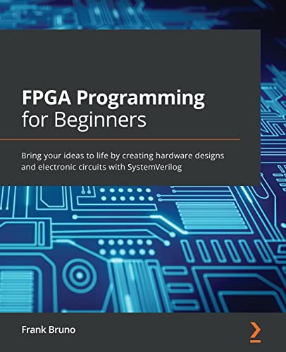
Those are good. I have some articles from a few years back on my blog: asicsolutions.com. I also wrote a book on SystemVerilog that covers some of that: https://www.amazon.com/FPGA-Programming-Beginners-electronic-SystemVerilog/dp/1789805414/ref=sr\_1\_1\_sspa?crid=29UJ63HS2UKPB&dchild=1&keywords=fpga+for+beginners&qid=1622556840&sprefix=fpga+for+%2Caps%2C174&sr=8-1-spons&p...
Here are two books by the same author that I find didactically very good:
https://www.amazon.com/Quick-Start-Guide-Verilog-LaMeres-ebook/dp/B07PGQ2B3B
https://www.amazon.com/Introduction-Logic-Circuits-Design-Verilog/dp/3030136078
Depending on your interests, one or the other is more suitable. If you don't know much about digital design yet, I would recommend the second one (the first one is a subset of it).
Depends on whether you are doing verification out design. For verification, maybe the definitive work is: https://www.amazon.com/SystemVerilog-Verification-Learning-Testbench-Language/dp/1461407141/ref=mp_s_a_1_1?dchild=1&keywords=systemverilog+chris+spear&qid=1615613164&sprefix=system+v&sr=8-1
I can't recommend that verification book enough. It's excellent. Unfortunately, there just isn't as much high quality information online for systemverilog as there is for other languages. This book is an invaluable addition to my reference information, in addition to Google.
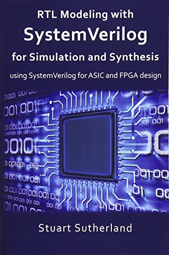
There is s newer book by Stuart Sutherland that I don't have that might combine concepts of simulation and synthesis. It is probably really good too.
Here are two books by the same author that I find didactically very good:
https://www.amazon.com/Quick-Start-Guide-Verilog-LaMeres-ebook/dp/B07PGQ2B3B
https://www.amazon.com/Introduction-Logic-Circuits-Design-Verilog/dp/3030136078
Depending on your interests, one or the other is more suitable. If you don't know much about digital design yet, I would recommend the second one (the first one is a subset of it).
If your issue really is the cable, you can just buy one (or a couple) for nothing on amazon. Anything like these would work fine. You can probably find a use for them anyway if the issue ends up being somewhere else.
Short answer, no, there is no cheap board with 4 network ports.
With that being said; you can buy a board with a single ethernet port, and a $25 managed switch, hack the NetFPGA code a little bit and configure the switch correctly, and you have a "4 port" FPGA.
yea, pwm output and then low pass filter. this page has a good description of the process and why it does what it does. https://provideyourown.com/2011/analogwrite-convert-pwm-to-voltage/
I did the same thing a while back working on making a fpga synth. I'd also suggest just buying some 3.5mm audio jack components. They're worth having on hand regardless for fun audio projects. https://www.amazon.com/Uxcell-a12062600ux0366-Female-Stereo-Connector/dp/B008SNZUYC/ref=sr_1_2?dchild=1&keywords=3.5+mm+pcb&qid=1606631221&sr=8-2
Ashenden also wrote what I consider the VHDL Bible, so I would assume it's good. But I haven't seen any of this other books (nor this one since it had a plain green cover), so take my advice with a small chunk of salt.