
What are
/r/PrintedCircuitBoard's
favorite Products & Services?
From 3.5 billion Reddit comments
The most popular Products mentioned in /r/PrintedCircuitBoard:


The most popular Services mentioned in /r/PrintedCircuitBoard:
HackADay
Altium Designer
Snipboard
CircuitLab
Circuit JS
OLinuXino
SourceForge
Fritzing
gEDA Project
Alibaba.com
Hackster
Kickstarter
DipTrace
Chromium OS
BeagleBoard
The most popular reviews in /r/PrintedCircuitBoard:
You mean the $3000/seat price + subscription? That's for starters.
And if you really want feature comparison and are too lazy to google, you can find the list here: http://www.altium.com/altium-designer/features
Right of the bat, Kicad has none of the features on the first page alone.
Kicad isn't even playing in the same league. That doesn't mean it is useless - it can actually do very good job if you use it for what it has been intended for.
However, by comparing it with Altium you are attempting to compare a bullet train with a bicycle. Both are means of transport but that's about all they have in common. If you wanted a meaningful comparison with Altium Designer, you would need to look at e.g. Mentor Graphics products or Cadence.
It sounds like you are talking aboutsome sort of system not unlike the restaurant pagers that exist. I'm not certain if they definitely use a sprung pin (pogo) connector, but it makes the most sense.
https://www.amazon.com/Restaurant-Paging-System-Coaster-Lights/dp/B00B86HRLA
Export your files from your project and use a gerber viewer.
That will show you what the files look that you are sending away.
Your EDA does not look like something i am familiar with so i can give no advice on how to export them.
But i can give you the link to a gerber viewer:
https://sourceforge.net/projects/gerbv/
You can also use a online gerber viewer to share your files here instead of using screenshots:
http://gerblook.org/pcb/4PvJhVWPBAdkeunNm2Sjne#back
Your routing could be way better but is not the worst i have seen.
Try to keep more clearance between traces and try to avoid sneaking traces between pads.
Mounting holes are your friend, even id you do not need them.
Is manufacturing them yourself an absolute requirement? Or would you be alright with creating them and sending them to a fab to be made?
If you're alright with not making them yourself, you can use kicad which is a free CAD system for designing PCBs. And I would suggest hackvana as a manufacturer. He has very reasonable prices and takes care of things like panelization for you so you don't have to worry about it. You just give him your files, pay him, and he sends you the boards. He's also a super friendly guy.
Good luck! Sorry I couldn't help in terms of manufacturing them yourself, though it's much more involved and can be more expensive due to the extra equipment required.
A bit of googling: https://sourceforge.net/projects/gerbv/
There is not a lot to a gerber viewer, basically a gerber format parser and then a 2D polygon generator. Those you can then display in 2D or 3D.
3D board visualization is a different thing, for that you need more than just the gerbers. Typically you will want model files for the components too.
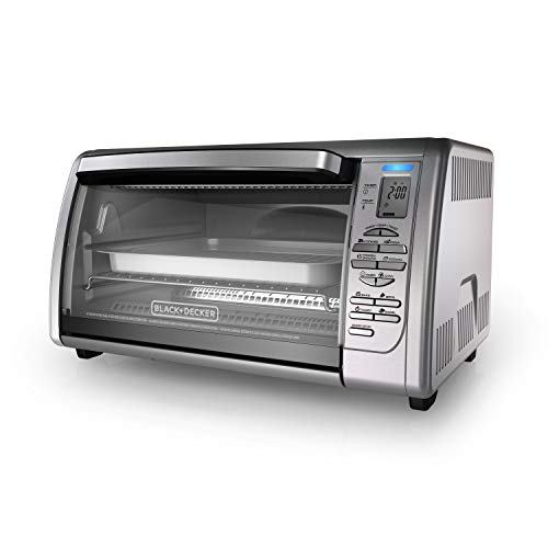
I bought a toaster oven and the ControlLeo Kit. But I haven't modded it yet. I just put the boards in and baked with convection... after about 4-5 minutes, they are ready.
Here's the oven I purchased on amazon: toaster oven
Check out PyCubed, its an open source cubesat project that has been radiation tested
http://roboticexplorationlab.org/projects/pycubed.html
https://www.notion.so/PyCubed-4cbfac7e9b684852a2ab2193bd485c4d
Just FYI,these do exist already... Here: user selectable voltages, etc. (They're also all over ebay and aliexpress, etc...)
I have a few of them. and they work quite well. Tested up to the 20V 3A so far. (I don't have a 100W PD charger to test with.)
That said if you're doing this as an exercise, then I'll let others chime in with the critique.
The only reason I could think of to not accept x-outs is if you're shipping the boards directly to another manufacturer who's going to mount them in the final product or something, and you don't want to cause confusion when there's 53 boards but 50 are good and the three are just random ones with a big X drawn in permanent marker. But breaking them apart isn't a hassle at all, especially when you're doing it yourself for a small quantity, I actually find it kind of easier to break apart a set of 10 than to remove each individual one from a bag.
The only thing to watch out for (a mistake I made the first time a vendor did the panelizing for me) is if traces are close to the edge of the board. Usually if they're routing the board out (like for a single board) it's pretty accurate, and they won't wreck a trace that's close to the edge. It's not usually an issue with V-scores, but if they use mouse bites (a series of small holes) as breakaways, I've had the PCB splinter a little and it ripped a thin trace off the board. It was poor design on my part, the trace was way to close to the edge, but just something to be aware of.
If you're looking for an excuse to buy a tool, I found these really helpful for breaking apart V-scores: www.amazon.com/Hakko-PN-2007-Long-Nose-Outside-Serrated/dp/B00FZPHEW2
And these for cutting mouse bites a little cleaner than breaking them: www.amazon.com/Hakko-CHP-170-Micro-Cutter/dp/B00FZPDG1K
But you can absolutely do them by hand. You wouldn't need any special tools unless you're doing thousands or something.
If you’re designing a board, you want to make sure you have access to pins 11, 12, 13, reset, gnd, and 5V. Typically send them out to pads or holes that are easy to access.
If you don’t have a board and you want to use just the chip, you can buy a “TQFP-32 socket” for $10-20. Here’s one on ebay. https://www.ebay.com/itm/1Pcs-TQFP32-QFP32-TO-DIP32-28-IC-Programmer-Adapter-Chip-Test-Socket-Pitch-Black/173689092477?hash=item2870ad397d:g:PD0AAOSwnDRcdo1U
Another option is to use a breakout board like this: https://www.amazon.com/dp/B07CJ96ZPW/ref=cm_sw_r_cp_api_i_j.joFbZ2946JD but these require you to solder them on.
Can you elaborate more on what you mean by trying to program it without soldering? Typically, you don’t prototype things with surface mount components. You’d usually design a PCB for them, which is why the ATMEGA328 comes in so many different footprints
There is a conductive ink pen you can use. Though I think I last saw it on kick starter so it might be vapor ware by now
Edit:
Kick starter ended. Orderable product now
http://www.electroninks.com/shop/
https://www.kickstarter.com/projects/electroninks/circuit-scribe-draw-circuits-instantly
Yes, I am aware of that. I am not saying you should buy a pirated clone, my point was that the chip is a pain in the backside even if it is completely original, because the hardware is so old.
If I needed an OBD II dongle, I would probably look at implementing the interface with a more modern ARM MCU, e.g. one of the STM32F0 or F3/F4 or NXPs LPC1517 series instead (for ex. this design: http://hackaday.com/2016/03/27/open-source-obd-ii-adapter/ ).
I have been playing with one of the (original) Bluetooth dongles using the ELM327, but the serial output was unable to keep up with the traffic in a 3-series BMW. However, it is possible that the BMW runs faster bus than 500kbps.
Also those dongles were poorly engineered - the output was fixed at 9600bps. The ELM327 permits to change the output speed but that doesn't change the speed of the Bluetooth interface - effectively bricking the device if you attempt it.
I have two questions:
1. What would you recommend for adding Bluetooth to a PCB for production of 200-2000 units? I'm looking at ordering an SMD module like this one. I'm using an older version of BT due to my app compatibility. Are these modules pick and place compatible?
2. What would be the most cost effective way to have three 3-wire JST SM connectors coming from the PCB? Cost is the most important factor here, whether the connectors are directly on the board (which I don't think exists), there are fixed wires coming from the board with connectors, or if there is means to attach the wires to the board such as screw terminals it does not really matter. I want to have JST SM connectors because these are the most common for WS2812 LED strips.
> what i dont understand is how can a companny acquire open-source that is openly contributed ? i mean if i make a module in mysql ( when it was open-source) wasn't that source my rights to be ?
MySQL in particular is GPLed, but is also available from Oracle with a proprietary commercial license. Oracle can do this because they require all contributors to sign the Oracle Contributor Agreement. With the OCA, every contribution is jointly owned by the contributor and Oracle, which gives Oracle the right to relicense the code.
The OCA contains wording that contributions will always also be licensed under an FSF or OSI-approved open-source license.
I don't know how the licensing was before Oracle, but I do know that the project was always maintained by a company (starting with the inventors MySQL AB, then Sun, then Oracle) and probably always had legal provisions for dual-licensing.
Another example is Nginx, which is commercialized by the founders' company Nginx, Inc. Because the open-source Nginx code base has a BSD-like license, everyone can commercialize it. Nginx, Inc., besides contributing to open-source, develops additional proprietary functionality and combines it with the open-source basis into Nginx Plus.
Going back to MySQL, it's IMO a perversion of the GPL's somewhat "anti-capitalist" spirit, because it practically prevents anyone from commercializing the code except for Oracle, who can commercialize however they want because of the OCA.
Well, MariaDB is doing the same thing with the MCA.
I don't want to be negative, but: http://hackaday.com/2016/10/11/creating-a-pcb-in-everything-friends-dont-let-friends-use-fritzing/
Switching to a more industry-standard ECAD program should be done sooner rather than later. KiCad is a great (and free!) package.
http://hackaday.com/2016/06/02/tools-of-the-trade-reflow/
We've used the hotplate method for runs of hundreds, and an off the shelf toaster oven for thousands. You can get by without even modifying some toaster ovens and using things like the "frozen treats" button if such a thing exists. I've used the Controleo mentioned in other comments, but I've also used an oven on just the frozen treats setting and the only thing I did was hack the convection fan to permanently on because the treats setting didn't use it.
I wrote this a couple months ago. http://hackaday.com/2016/06/29/tools-of-the-trade-inspection/
I'm working now on a followup article to be published next week which goes into more testing and programming tools.
Other than a lot of functional testing is done with special test jigs which have custom hardware for probing and testing the device. I've also developed test jigs which do calibration and testing, so they go in a special controlled chamber where certain sensors are calibrated. During this process I also issue commands to the microcontroller that run various self tests and report back. You can do all kinds of fun stuff with test modes on PCBs, for example executing a special input which puts the device into a test mode and lights up an LED if the self test passes/fails.
I downloaded every one of my invoices from Digikey about a month back to give me an easy way to search for components I had previously ordered (it's easy to overlook you have those 100 .1 uf capacitors sitting in a box somewhere) - I purposely did not tally the totals because I wasn't willing to face that demon just yet...of course it took all of 5 minutes for one of the guys in our tinkerer facebook group to tally the total and throw it in my face...
Those $5 and $10 orders totalled something like >$1,500 over a 3 year time span (Yes I purposely forgot the exact amount).
Anyway - have a funny saying in our group.
"Why buy it for $30 when you can build it for $100?"
It sounds stupid and pedantic but I can honestly say after 3 years of tinkering and learning this stuff - you can not put a price on the knowledge you gain from every project.
My daughter thinks I'm a wizard because I can fix literally anything that breaks (which at this point is mostly toys). Missing a gear? No problem 3d print it, busted capacitor? no problem I have a steady stock of replacements... and of all the toys they love - the one they get the biggest kick out of is the "useless machine".
Anyway sorry for the tangent - the board took me 17 hours to solder because I didn't know what I was doing at the time... that same board takes me 15 minutes to assemble today using cnc stencils and reflow ovens.
FYI this was the hackaday video that gave me the idea to apply solder paste using a toothpick.
Edit - if you need help with recommendations on interesting stuff to have on your bench just ask away...
Other ppl have already answered your question, but just another FYI, not all board houses can make plated slots (ie, OSHPark.com, my favorite board house). So you may have to shop around if this is something you absolutely have to have.
And then there's this, if you're just looking for best price http://hackaday.com/2013/01/30/finding-the-cheapest-board-house/
I haven't used Diptrace myself, but the feature to move changes to/from schematics does exist:
http://www.diptrace.com/forum/viewtopic.php?f=3&t=9396
You will save yourself a lot of troubles with the layout if you use SMD and not through hole caps for the decoupling capacitors.
The routing mess you are having is because you aren't using a copper pour. Once you do, the caps will have one side sitting o n the copper pour (which will be ground) and you don't need to route tracks around them like that. Seriously, if you are planning to etch that at home, do use a copper pour - if for nothing else then to save you etching time and etchant!
See here how to do it: https://www.youtube.com/watch?v=5bMT8EETyrk
Usually via sizes are chosen for their signal characteristics (inductance, power handling, etc) as well layout density comes into consideration as well when using different drill sizes.
That said, if you have no hard requirements on the via hole size you have a few options.
As the easiest option, design the PCB as you would for production with a PCB fabrication house. When fabricating the boards yourself, once you create the technical toolpath you should be able to override the required drills with the ones you have available. Using the largest drill you have in the tool magazine which is less than the hole diameter as an override.
Another method is to design normally for production PCB fabrication and then create a variant where you use the "PCB" window to query/select matching all vias and then the "PCB Inspector" dialog to manually change all matched vias to the size you'd like to use.
The 3rd option is to change the default via size in the PCB Editor section in preferences.
The 4th and 5th options vary depending on your routing style, if you route vias interactively or manually. If you route them interactively, you can edit via sizes in the "Favorite Interactive Via Sizes" dialog, which is also found in the PCB Editor preferences. If you route them manually, you may use the "Choose Via Sizes" dialog, which you'll find more info in the online documentation: http://www.altium.com/documentation/17.0/display/ADES/PCB_Dlg-FavoriteInteractiveViaSizesForm((Choose+Via+Sizes))_AD
This, although it seems that many are not willing to spend...
I quoted someone $15k for schematic capture + PCB layout of a board on the below level of complexity over a month term (which comes out to around $94 at 40hr/week but I saw it taking a larger commitment of time at maybe 60hr/week) and was ghosted lol. People aren't willing to pay for the knowledge of designing boards like that while accounting for DFM, DFA, FCC/CE, etc.
https://www.olimex.com/Products/OLinuXino/A64/A64-OLinuXino/open-source-hardware
This is the recumbent bike. The control module is battery powered (4xD Batteries) and it functions with multiple membrane buttons, while displaying simple information to a little screen. It also tracks heart rate monitor handles.
Here are the pics of the boards + damage in question
The battery springs/contacts were rusted to shit, but I know I could replace those for a couple of bucks.
OK. Coupla options...
- Flux the braid.
Do you have a solder sucker? This might be the job for one. https://www.amazon.com/EDSYN-The-Original-Deluxe-SOLDAPULLT/dp/B006GOKVKI
- I'm not generally one to publicly advocate desoldering by the 'sling method', but heat the solder and quickly swing it in a wrist-motion like you were trying to shake off a spider that crawled onto it. Or tap it against the workbench to smack off the molten solder.
- I'm not generally one to publicly advocate desoldering by the 'sling method', but heat the solder and quickly swing it in a wrist-motion like you were trying to shake off a spider that crawled onto it. Or tap it against the workbench to smack off the molten solder.
Don't tell anyone that I told you to do that. Though we all have. A lot. And NEVER do it in an electronics classroom environment.
This module appears to contain both the camera interface and SD in a fairly small package:
https://www.amazon.com/HiLetgo-ESP32-CAM-Development-Bluetooth-Raspberry/dp/B07RXPHYNM
When you're doing hardware development on something brand new, the first step is usually to buy a development kit or otherwise working version of the thing you're trying to integrate. That way you have a known-good point of reference for when you do both the software and hardware design (and there will be a lot of software design).
Another choice is to just simply buy a module like this and slap it directly into your design, board and all. There's no shame in that and it will save you a lot of headaches. If you can avoid it, don't reinvent the wheel if there's a cheap, easy solution already available. Especially for a graded project.
Save reinventing the wheel for your personal projects. That's how we all cope.
Appreciate that! I ended up getting this one after getting annoyed at myself for looking at toaster ovens all day.
From what I read you can also play with the booster element placement to make up/fix those hot spots?
Look for 1N5818. They should be pretty much interchangeable, unless you need oddball high reliability or mil-spec versions.
Digikey is sold out of the Fairchild version, but has several others available.
Newark claims to have it in stock from onsemi.
What continent are you on? Taiwan Semi has them for $0.073
Ok,
So I tried to measure a 3d printer board (with atmega2560) directly at the XTAL pin and it gives me 16mhz, so the scope is working as expected.
When trying to probe the XTAL on the board it doesn't give me anything (apart from the 60HZ that I get on all pins).
As I mentioned, I've manually tied the RESETEN and run to GND and VCC and still nothing.
The board is supposed to work out of the box with USB according to what I read online, that's why I didn't exposed the JTAG ( and also since there is no room for it lol (check the board pictures)
I'm adding the schematics and the board view to my main post so you don't need to search this comment.
The solenoids are an Amazon fine. I really liked the 1 in, 4 out in a single molded component, saved me having to build my own manifold.
Here is the link:
If the board is single sided, I recommend a hot plate, like this one: https://www.amazon.com/Soiiw-Microcomputer-Soldering-Preheating-200X200mm/dp/B083Z38S9P
That'll get hot enough to melt bismuth solder, and it'll warm up other solders enough that you won't need to hit so hard with the heat gun.
Get a toothbrush and container of >90% IPA to clean them after soldering.
You can get cheap stencils from OSH stencils (https://www.oshstencils.com/). Stencils are nicer than doing it by hand.
I'm not sure that doing more than a handful is a good use of your time. If you're doing a hundred, it's almost certainly worth it to send the boards out to an assembler once you know the design is good.
Hi! In order to simplify the soldering process with hot air or oven, I prefer to use pastes composed of an alloy of Bismuth and Tin, they allow to have lower melting temperature compared to almost pure tin pastes. For example, chipquik one are my favourites, here is an Amazon link.
For what it's worth, I don't own a scope, but sometimes use a cheap logic analyzer. Sometimes it's enough to debug issues, and is significantly cheaper than even a cheap scope.
I use this one which is compatible with PulseView
Not to say you shouldn't get a scope, especially if you can afford a good one. I've just managed to scrape by so far without one :)
$5 toaster oven from Goodwill, $20 thermocouple probe (https://www.amazon.com/dp/B019GVKRE2). A small metal sheet to more evenly spread the heat.
Preheat board to 90-120C for a bit, then crank up to about 200-210C. Dwell for 30 seconds. Turn off and open door.
Have done hundreds of boards. Works fine for prototyping.
For magnification I use a flip-down visor like this. I have a microscope on my list to buy but haven't gotten there yet.
I keep my paste in a fridge and it seems to hold up pretty well over time; I've used paste that is months old and it has worked fine. I would buy new paste for production work.
I keep all my parts for all revisions of all projects in one box :P
I’m finally getting enough different parts that a better organization system makes sense. My plan is that “standard” components like LEDs, transistors, and passives will go in this with labeled bins and odd parts will go in a few unlabeled bins at the bottom.
What’s your workflow like? Do you need to maintain a few revisions for each of several boards, and it’s helpful to keep things organized by version?
thank you again. Unfortunately, i can't seem to find ferric chloride with any reasonable price.
its all liquid and its costly.
would %6 Hydrogen Peroxide do the trick?
thats also the highest Hydrogen Peroxide % i found around.
i want it to look nice but i guess i have to settle with passable grade if needed i guess.
Use a contact cleaner that is good at removing oxides to get the copper shiny again, something like this.
Once it is dry, apply a varnish that can be soldered trough. Don't wait for too long, otherwise the copper willl start to oxidize again. SK-10 is an example.
Not sure what how it is called in English.
I'm using a 4W 450nm laser, focused to a .1 or so mm dot.
It's on a 3018 mini CNC style machine. If you're using one of the belt driven laser engravers, slow it down and you'll get better results, though yours is looking pretty good for through hole stuff.
Just FYI, you should look into SMD..its vastly less expensive and once you learn how to reflow, it's a lot easier.
https://www.amazon.com/AideTek-BOX-ALL-resistor-Organizer-antistatics/dp/B0187S6CLM/ ESD version is better for smd
if you do end up going pick and place machine, the best place to store are on reels and use reel holders, unless you're doing the manual verison
Want more complex and no microcontrollers?
What about this? http://hackaday.com/2017/03/31/jaw-dropping-ic-free-pong-on-an-oscilloscope/
The design files are available: http://www.glensstuff.com/pong/Oscilloscope_Pong.pdf
lasers: http://hackaday.com/2013/11/26/laser-wire-stripping/ hot wire also works. there are a number of commercial flat ribbon cable strippers. Weidmuller makes some, as well as this nice video from jokari https://www.youtube.com/watch?v=7xA4LxdTRBY
You can actually just use a Dupont connector kit to make the connector. No soldering required.
Ok now I get it. That board is a power source for a camera. And the camera's power input is a usb cable.
There are ready cables for that, like this https://www.amazon.in/BiiYo-Female-Power-Charge-Connector/dp/B07KM69YVC#
But if you can refurbish an old extension then better use that.
No need for jumper wires. Cut the cable. Remove the black insulation for about 3cm. Cut the green and white wires (data). Remove 0.5cm of insulation from the red and black wire. Add solder tin to exposed copper. Slide a shrink hose over the wire. Solder the wire directly on the male header or optionally to a female header. (Bonus round: realize that you forgot the shrinking hose and remove the wire again, then repeat with shrinking hose.)
What do you need a PCB for when making a portable retropie? I'm guessing you mean this: https://retropie.org.uk/
​
In order to make this portable, it seems like the only thing you would need is a battery?
It looks like the CSR BC417 is a very popular BT chip. After looking into it more and trying to find suppliers it seems like buying assembled HC-06 modules might be more cost effective. There are many options for HC-06 modules that could be soldered onto my PCB like a SMD component. http://www.alibaba.com/trade/search?fsb=y&IndexArea=product_en&CatId=&SearchText=hc-06 Like what I got from Amazon but not mounted on the additional breakout board with pins.
/u/R4N63R
>Car makers have used this hack for steering wheel mounted buttons, i.e. cruise control, climate control, stereo control, etc., for a long time. It means only one pair of wires needs one clock spring to bridge from the dash to the rotating wheel.
from the comments on http://hackaday.com/2012/03/02/r2r-ladder-connects-multiple-buttons-to-one-adc-pin/
So apparently they use it to reduce the pin count when transmitting the data back to whatever processor, since I guess it's expensive/impractical to add too many wires to the rotating wheel. Unless you put some sort of 1-wire digital chip to translate the data before being sent to the main processor, but that would end up more expensive (a shift register would require 1 data and 1 clock minimum unless you did something fancy).
If he's retrofitting an existing steering wheel, I guess he has no choice but to use what is already there.
Hi, I took a look at your design and posted my notes in a pdf for your previous design (update 3),not sure if you saw it, but it seems like most of the notes there might be still relevant. It's only for the schematic part, I'll try to take a look at the PCB tommorow
A solder reflow oven, which is expensive as fuck. https://smile.amazon.com/gp/product/B01MR2IWBN/ref=ppx_yo_dt_b_search_asin_title?ie=UTF8&psc=1 is what my buddy had me buy when one of the leds on my pcb was installed incorrectly.
Here's a similar product you could suggest to customers while you sort out supply chain issues?
I'm not really feeling like I'm being helpful by sharing this.
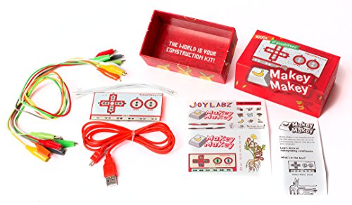
https://www.amazon.com/JoyLabz-MMCE-Makey-Invention-Everyone/dp/B008SFLEPE
​
Are you looking for a contractor? I don't really think you'll be sharing your BOM here out in the public for the world to critique? And you probably aren't about to open source it.
Thank you for the advice. Your general process seems similar to mine. I can't imagine trying to do a layout before actually having it breadboarded, but I haven't made the transition to SMD yet, so it is easier for my projects.
I've heard the Arduino story before, and I'm not sure how much I believe it. I'm sure it was an honest mistake, but thy clearly weren't too interested in making it more user friendly. I'm also perhaps a bit salty since Arduino has a lawsuit against itself (kind of, more details in the link) over being open source or making profits.
Soldering iron with the knife tip where you place the tip along the length of the component or use two soldering irons with a point tip and heat both pads at once is the easiest way to do it.
Hi guys, thanks, the only problem is that I couldn't find the right inductors I need to create a switch power supply that wanted LM2596.
So what I decided to do is to cheat a little and just use a ready LM2596 module (from amazon) and install it on my PCB.
It can handle 3 amps and it's pretty efficient and easy to get (already ordered).
I actually searched the part you sent on amazon and it's around the 30$ mark! crazy.
I don’t see any reason the fuse you listed wouldn’t work, but if this were my project, I’d probably use an inline fuse holder with a standard automotive fuse on the line in. Like this: https://www.amazon.com/dp/B07WVXWDXL
Can confirm, I got this one from CAT and it's great. "Loud refrigerator" is spot on.
There's also SilentAire which are way quieter but also $$$$.
What does that mean in practice? I've been going off of my best understanding of the USB C specs, like how they are described here (https://www.chromium.org/chromium-os/cable-and-adapter-tips-and-tricks) specifically what they note as being in Section 3.6.1 and 3.5.2 of the official specs.
Thanks for the response!!
Whenever I convert it to a pcb, the grounds always become an issue. Instead of the ground pins being labelled as GND, they say p1_04 or something similar, and the grounds wont connect.
> https://www.youtube.com/watch?v=J9Ig1Sxhe8Y
I watched this exact video yesterday. Still wondering the best steps forwards.
fivrr:
https://snipboard.io/hiHUed.jpg
Says he doesn't need the schematics to continue (?)
> I can't find another vector graphics software that can import DXF files.
Inkscape will import DXF.
Even better, there are 2D CAD software available for free: Draftsight (https://www.3ds.com/products-services/draftsight-cad-software/free-download/) and DoubleCAD (https://www.turbocad.com/content/doublecad-xt-v5) for example.
When using DXF's, try to use the oldest version DXF possible for the best compatibility between programs.
Hi. You can use KiCAD to get a PCB design from Gerbers files.
Then, you can use FreeCAD to get a 3D model from the PCB generated with KiCAD.
But only PCB, no components.
Import Gerbers to KiCAD (gerber viewer -> pcbnew) is easy. Then you get a PCB file that you can use to get a 3D model, but if you want a detailed model... maybe this is not useful. This way you get a model of PCB only, with drills, but without components.
Your PCB looks great, but I'd recommend using Inkscape (a free vector graphics program) over excel for the prototype board. It's pretty easy to use and since it's intended for drawing it has more features that are handy for drawing layouts like layers for example.
Googled some of the file header and the source file linked by OP in comments is from gEDA.
​
See http://www.geda-project.org/
​
The big tip that the file wasn't Altium is that it wasn't a binary blob on GitHub.
You have the right idea -- what you do is to create locally defined items in the BOM catalog tab -- (http://www.altium.com/documentation/17.1/display/ADES/((ActiveBOM))_AD#!ActiveBOM-LocalPartCatalog), creating entries for your enclosure and for the manufacturing step for the enclosure modifications.
Then you add the catalog entry into the BOM components tab so that it becomes a part of the BOM.
Then in your output job, you generate the output BOM with the BOMdoc as the source file.
Just use "place holder" for the enclosure, and "process" for the machining.
Altium do have a free edition, it's fairly new. http://www.altium.com/circuitmaker/overview I haven't used it myself, I use the full blown version but it might be worth checking if it can edit the Altium files provided.
I'll have a look this evening to see if it's possible/practical to open the Altium project and save as Eagle.
As others have said, starting something like this from scratch is a very difficult task, even for those with experience. What you can do though is take an existing open source hardware design and customise the layout and connectors based on the capabilities of the ARM SoC (System on a Chip) processing unit.
Olimex produce a large number of SBCs that run Linux (and others). Check out their page here. There are other manufacturers that also open source both the hardware design and other important things like bootloaders. Even if you build a board such as the RPi, it will be useless without these normally closed source pieces of firmware, etc.
Even with all these resources at your disposal, it's very likely your first SBC will just not work. They are crazy complicated, and if you don't yet understand things like Ohm's Law and other electrical/electronic engineering concepts you may never get it to work. There are courses available online to learn everything, with sites like Pluralsight (get a 1 month free trial by signing up as a Visual Studio developer over here), Lynda/LinkedIn Learning all offering free trials that will give you enough time to learn so much.
The CPU on the Rpi doesn’t support parallel flash or SATA. The options are a bit limited to an SD card or an USB stick. A USB to Sata converter is possible but hard to design yourself.
If you want something like an Rpi but with Sata have a look at something like this: https://www.olimex.com/Products/OLinuXino/A20/A20-OLinuXino-MICRO/open-source-hardware
It's somewhere in between an Rpi and an Rpi 2 in CPU speed, GPU speed is also not too bad and it supports SATA for an HDD or parallel flash. This is a version with 4GB of onboard flash: https://www.olimex.com/Products/OLinuXino/A20/A20-OLinuXino-MICRO-4GB/open-source-hardware
The PCB and schematic are open source and made in Eagle so you can download them and have a look inside them and they even sell the CPU separate, although soldering a 256 pins BGA is challenging :)
It is the same situation if you would just unplug the AC input. There would be no current path and your caps would slowly discharge, turning the 7805 and 7809 off. You can easily simulate such scenerios, for example on http://www.falstad.com/circuit/
By the way, I just noticed that both your Schottky diodes are placed in wrong direction. :)
I was bored. https://gofile.io/?c=jA5suM
This is a very quick & dirty routing job. By no means did I check if everything was ok. Tried to pay a little attention to uniform routing of the cols & rows, and somewhat better placing of the caps around the MCU.
And no, I did not bother creating screenshots. There's pdf's in the link.
Quick steps is to download github desktop, log in and create the project there with Add>Create New Repository, and select the existing arduino project folder.
Once it's there, you'll see all your files haven't been added yet to the git repository. Press the green [+] on each file/folder, then enter a quick summary and optional description and press "Commit", then push repository menu->push.
Literally just something like this? I know it looks super simple but there is quite a bit going on to be aware of.
PCIe and data transfer at those speeds is going to require specific stackup, materials, impedance controlled traces, manufacturing call outs for gold finger edge specs, chamfers, etc.
I'm literally wearing a Robert Ferenc shirt as I type this and more power to you, but with some of the questions you are asking I would be concerned particularly if you want to get full on 16x GPU gaming kind of performance and run it though your beginner PCB design riser card. 4.5cm are not necessarily short traces at nearly a gbps per pcie lane and there is a lot to learn and it sounds like this isn't something really are needing to dive in to and understand but just a means to an end for your project you otherwise are invested in. Look at outsourcing, even fiver or somewhere to find a pcb person.
If you do want to learn, or insist to do it yourself you are right, it isn't complex per se and I'd say you should just lean into a good board shop that could hold your hand through the process and give you a good stackup or template or help with the process. They'll be your best bet to get it done right. If they give you a good simple stackup, trace widths to design to (the pinout is easy enough and templates abound) they will be the ones doing the vast majority of the heavy lifting to get it right.
Thanks for the info! I picked up Test Driven Development for Embedded C and Unit Testing Principles, Practices, and Patterns recently and plan to work through those once I finish my Udemy course. Not sure if you're familiar with either of those. Do you use Linux or Windows on your laptop? I haven't looked into whether the STM software works on linux.
Why do you need A3? I don't think you will find any so big.
Are you trying to do A3 sized boards using toner transfer?? That's a bit insane, IMO. The quality will be terrible due to the uneven toner coverage and dimensions warping over such large area. That would really be the moment I would step back and reflect on what I am doing and whether it wouldn't be easier and *cheaper* to pick another production method or to have the board made.
Considering toner transfer paper, there is the brand name Pulsar paper which is expensive. Or just get the cheap generic yellow stuff:
But even regular paper will work, you may also experiment with printing on cheap vinyl sheets (the self-adhesive kind), that, when done right, will result in very sharp and clean transfers.
Wow thanks for the long reply. This is the 5v regulator I use https://www.amazon.com/gp/product/B07DYXTX9H Smoothing out rapid motors isn't really possible because of how the robot translates. The robot doesn't use an IMU because they don't work at the speeds I need, the accelerometer is mounted off center (only off center in one direction) to fully utilize it's range of detectable g forces. I have run without any leds before and there was no change in how long the electronics kept alive.
If you're talking about JST SM connectors (like these) no pcb headers exist for them.
I ended up not liking any solutions for this same problem and just ended up using terminal block spade connector thermocouples and build the mounting screw connections ight on to the board.
Awesome! That's great info thank you!
As for the flashlight. It's the real deal! Cured the resin in less than 20 seconds for me. Here's a link to the one I purchased.
https://www.amazon.com/dp/B01A5KLUG2?ref=ppx_pop_mob_ap_share
Any reason you need them straight like that or would right angle work?
Although they do make right angle male headers, so...
I think you are right about the temperature issue. I just read through several forums that mentioned this happening with brother printers. I'm certain this was transfer paper. The reviews are pretty good, too. Apparently I'm not the only one to have this problem, though. The 1star review says similar.
https://www.amazon.com/dp/B07MYXK4WJ/ref=cm_sw_r_cp_apa_fabc_Kd-7FbZEY1FJZ?_encoding=UTF8&psc=1
yeah, don't obsess over it I've done hunderds of boards in my oven just by switching it on and off with a power strip and watching through the glass. if you want a bit more control can add a power adjuster like this:
https://www.amazon.com/Lheng-High-Power-Electronic-Thyristor-Thermostat/dp/B07S3LZ4H9/
I am guessing you are just using a regular 3x3 grid to display your tic-tac-toe.
If I were you, I would be using a dual color led, so red and green in the same housing.
Something like this (very quick find just to illustrate)
There are also other bi color leds available if you prefer. But by having them both in the same housing it will make the 3X3 grid easier readable and structered.
​
You might also want to add some hardware push-button de-bouncing to prevent multiple entries being counted, this could be done in either hardware or software whichever you prefer there is plenty of info available if you search for button debouncing :).
So...this is weird. I stuck diodes on the GPIO pins connected to the U1/U2 inputs and put 1/4W 500 ohm resistors in place of R10/R11. I was charging and discharging both caps just fine, did it about 10 times. Then I hooked up the IR sensors and during the first charge cycle I saw a spark near the IR sensor headers on the PCB and my ESP blew again. Upon further inspection, I found that the 2nd IR sensor blew up (specifically the IC on the sensor module became a short). This is also not the first IR sensor module to die strangely.
The IR sensor in question is https://www.amazon.com/dp/B07F1R2DJ3/ref=cm_sw_r_cp_apa_fabt1_u7OSFb131SQ2Z
The only thing I can think of is that a voltage is somehow being induced into the IR sensor cabling, but I wouldn't think that would be possible. The IR cable is not going near the high voltage charging lines. But it does run along side the 12V line, which can carry over 1A of current. Both lines are about 20cm long or so, but are only next to each other for about 10cm.
Please....I am begging....this is driving me nuts. I am so lost.
https://www.amazon.com/dp/B07PGMBG1Q?ref=ppx_pop_mob_ap_share
Don't know if that link works, but that is my high voltage source. It is a ZVS boost converter that is current limited to 200mA. The coils have fly back diodes to suppress the back EMF.
If you need a straight cut across a PCB and don't have some of the tools that other people recommended, then you can score cuts on both sides of a PCB then snap it apart into 2 pieces.
1) Prepare
Find a piece of plywood or piece of lumber that you can sacrifice for cutting purposes.
Find a straight and sturdy piece of metal, or metal ruler.
Find a sturdy sharp "carpet knife".
Find a couple of plyers and some tape.
2) Put the metal on the PCB, with one hand push down on the metal with lots of pressure to prevent the metal or PCB moving , then cut along the edge of the metal. Repeat multiple times.
3) Use knife to cut a small groove on both edge of PCB at the same place you cut the PCB.
4) Flip over PCB, line up metal edge with cuts on the edge of the PCB, then repeat similar as the first side.
5) Get 2 plyers, then put multiple layers of tape over the jaws to prevent it from leaving marks on the PCB, or use rubber/plastic or something smooth to cover the jaws or buy plyers have have software materials on the jaws.
6) Sqeeze the 2 plyers close to the score lines that you previously cut, then twist the plyers to snap the PCB.
7) Use a file or sandpaper to cleanup the edge of the PCB, but don't breath the dust from it!!!
8) Good luck!
I second the YiHUA rework station. Got mine from Amazon. Has worked well for my hobbyist-level projects over the past few years.
For a two layer board, you generally have a ground fill on the top and bottom. You want ground to be continuous and as close to your signals as possible. The boards start off covered in copper before etching, so you might as well use that copper for something.
This book explains why you want to do that quite nicely, but in general it's because
- You want ground to be ubiquitous - you don't want one component to have a short, low impedance path to ground while the other has two wiggle through several inches of traces with a lot of interference, because those two components will have different ground references... which is bad (that part is usually pretty obvious)
- The energy of a signal is actually in between the trace itself and the reference plane (ground). Because the field is taking up that space, you want to keep it happy and contained from the origin to the destination. If you have one ground trace on the other side of the board, all of that field energy will co-mingle and create "cross-talk"
Does your board *need* those planes? If it's just a low speed, simple circuit... probably not. If you want to know what best practice is and why, there ya go
Also for a deeper dive, the go to text on high speed signals is Johnson and Grahm.
If you do not have a flux pen, invest in one.
https://www.amazon.com/dp/B005T8OR4I/ref=psdc_8107037011_t1_B0819YHJPJ
It's like a felt-tip pen, but with flux instead of ink. Get the flux flowing by pressing down on the tip.
When you use solder wick, pre-soak the wick with flux first. The wick will work much better. MUCH better.
If you have a solder joint that looks bad, soak it with flux and touch the iron to it. It will clean right up. Dull and scaly looking solder has reacted with oxygen in the air to form brittle (and non-conducting) oxides. In the parlance, this is a "cold solder joint." Flux reacts strongly with oxygen (particularly when hot), "stealing" it from the metals and thereby reducing them back to purity.
To expose a track, scrape the soldermask off with the edge of an X-Acto knife. Scrape lengthwise along the track, not sideways. Once the copper is exposed, wipe flux across it, then tin it with solder.
To tack a wire onto the track, start with the track tinned and the wire tinned. Flood the track with flux. Cut a short piece of solder (1/8" or less) and lay it alongside the exposed track. Place the wire onto the track surface and hold it in place with tweezers or small needlenose pliers. Clean the solder tip thoroughly, then touch it to the piece of solder and drag it over to the wire/track joint. It should solder the two pieces together immediately.
Isopropyl alcohol makes great flux remover. You can get it from Amazon also. Get the anhydrous (99.9%) stuff, not rubbing alcohol.
These are not 0.1" standard headers. I know because I tried to use 0.1" standard header compatible jumper wires in an attempt to spiff up my son's PC with ARGB LEDs and then realized it wasn't going to work.
If you can easily get your hands on low-temp solder, you should do that, as it will make removing the damaged header easier and will be easier to remove the old solder with a pump. Then use a replacement header (Amazon has some ARGB connector kits like https://www.amazon.com/Alphacool-Y-Cable-4pol-Connector-Black/dp/B07DF3JF16 for example).
Indeed when I go to my order history on amazon now and click on that item, it says "unavailable". The model number was TO1303SB. The amazon item code is/was B00FN3MV88.
When I look around now, the TO1313SBD model looks close/identical to me: https://www.amazon.com/dp/B07K1LSGXL.
Basically, one of these. Makes it a lot easier to repeatedly align the stencil with the board. Even doing a single board is easier, and you get better stenciling.
i've been running all pwm-applicable projects for years using these boards, which is where i sourced these particular components. i took this configuration directly from them.
they're some of the only mosfets i've used that have almost no noticeable heat dissipation (while others necessitate heat sinking.)
15Amps/400watts seems more than adequate for any application so far.
i would be running PWM at just above the range of hearing, ~20KHz, to avoid the harmonic resonance whine in the 12v power supply.
​
do you have any suggestions on how i could get a clean power source with step-down conversion?
​
and, yeah, sorry about the ground. since everything terminates into a wire terminal, i wasn't sure how to annotate the ground explicitly. i should have at least color coded the nets.
You can mitigate a lot of problems with a drop liquid flux from a needle tip bottle. A better iron will help too.
This $12 listing for an ESP8266 (an Arduino compatible MCU) with relay built in has a schematic in one of the photos: https://www.amazon.com/WHDTS-ESP8266-Channel-Transmission-Distance/dp/B071WWMMDD
If you're looking to learn how to make a PCB, it's a good project. If you just need an arduino with a relay on the same board, check out the link above or just search "ESP8266 relay" on your favorite site for 1, 2, and 4 channel versions
The photo resist commonly used on PCBs has its peak sensitivity at 395nm. You can actually by strong LED lamps at that wavelength. (https://www.amazon.com/dp/B07922NG1C/ref=cm_sw_r_cp_api_i_sCCgBb3K7EX8R)
However, the sensitivity goes down below and above fairly slowly, so e.g. 405nm works still very well. I for example, use a laser at that wavelength.
it would need at least detailed sharp, pics of both sides of the board and clear picture or schematics of the wiring.
OTOH, you do get what you pay for. Is $60 too much for being sure that your house doesn't burn down because of a cheaply made junker? Fixing the problems in the cheap one would likely cost more than that.
Finally, a much better solution than these chargers is to buy a normal fast charger for 4-8 AA cells. Some of those chargers will charge a pack in 60 minutes, there were even some that did it in 15 (but those needed special type of NiMh cells).
E.g. something like this: https://www.vapextech.co.uk/fast-smart-charger-for-1-8-aa-or-aaa-nimh-batteries-lcd-display-vapextech/ That has both fast charging, detection of a faulty battery and trickle charge maintenance, so that the batteries are always topped up and ready to go. That is vastly more capable than the charger you have found and costs about the same.
Or this one - a bit more expensive but the charging time doesn't increase with the number of batteries inserted: https://www.amazon.com/Powerex-MH-C800S-8-Cell-Smart-Charger/dp/B000LQMKDS
Yes, I get it that replacing batteries is a pain in the backside compared to just plunking the remote on a charger but you get much better life out of the batteries by separately charging each cell.
If you're looking at crimping (and I'd also recommend it) don't waste time trying to crimp with ordinary pilers, that's a one-way road to tearing your hair out.
The vendor recommended crimping tools are typically very expensive but you can pick up generic crimpers on EBay, something like https://www.amazon.co.uk/quality-universal-crimping-Japanese-Engineer/dp/B002AVVO7K I'm not recommending that specific seller, they're just the first one that came up in Google. Search for "PA-09 crimping tool"
The books referenced by the most presenters and PCB design conferences are Right the first time by Lee Ritchie http://www.thehighspeeddesignbook.com/ Highspeed design: A handbook of Black Magic - Howard Johnson https://www.amazon.ca/High-Speed-Digital-Design-Handbook/dp/0133957241
Note that A handbook of black magic reads like a text book, it is very long and very boring. The subject of PCB is complicated and requires an in depth understanding of the physics because just knowing the rules isn't enough convince other engineers that it's the right way to do something. More importantly, in my experience PCB design is always the least bad solution, you have to understand when you can break the rules and what the implications will be and understand if the trade off is acceptable
There are a million ways to screw up a layout, so I'd have to say yes but as a general rule? If you actually have your eyes open during the process and go in with some requisite knowledge, probably not.
Best recommendation I can give you is buy a good book on EMC, like Henry Ott's text. He even answers questions via email. Easily one of the best texts in my library.
http://www.amazon.com/Electromagnetic-Compatibility-Engineering-Henry-Ott/dp/0470189304/
Bruce Carter's Op Amps For Everyone has a surprisingly good guide to layout as well since op amps are, like most analog circuitry, quite dependent on layout. In fact, that portion of the text is so good TI reprinted it as an appnote:
google pcb design and pcb design decoupling capacitors
a lot of the manufacturers have good design notes available. if you aren't doing crazy high speed stuff, it's not too hard. high speed stuff requires the use of alchemy and black magic: http://www.amazon.com/High-Speed-Digital-Design-Handbook/dp/0133957241